In the television drama “Mission Impossible,” instructions for the mission were delivered on an audio tape that destroyed itself immediately after being played. Should that series ever be revived, its producers might want to talk with Georgia Institute of Technology professor Andrei Fedorov about using his “disappearing circuits” to deliver the instructions.
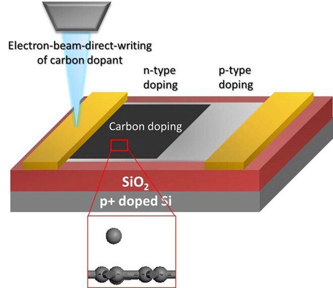
Using carbon atoms deposited on graphene with a focused electron beam process, Fedorov and collaborators have demonstrated a technique for creating dynamic patterns on graphene surfaces. The patterns could be used to make reconfigurable electronic circuits, which evolve over a period of hours before ultimately disappearing into a new electronic state of the graphene. Graphene is also made up of carbon atoms, but in a highly-ordered form.

“We will now be able to draw electronic circuits that evolve over time,” said Andrei Fedorov, a professor in the George W. Woodruff School of Mechanical Engineering at Georgia Tech. “You could design a circuit that operates one way now, but after waiting a day for the carbon to diffuse over the graphene surface, you would no longer have an electronic device. Today the device would do one thing; tomorrow it would do something entirely different.”
The project began as a way to clean up hydrocarbons contaminating the surface of the graphene. But the researchers soon realized they could use it to create patterns, utilizing the amorphous carbon produced via electron beam “writing” as a dopant to create negatively-charged sections of graphene.
The researchers were initially perplexed to discover that their newly-formed patterns disappeared over time. They used electronic measurements and atomic force microscopy to confirm that the carbon patterns had moved on the graphene surface to ultimately form a uniform coverage over an entire graphene surface. The change usually occurs over tens of hours, and ultimately converts positively-charged (p-doped) surface regions to surfaces with a uniformly negative charge (n-doped) while forming an intermediate p-n junction domain in the course of this evolution.
“The electronic structures continuously change over time,” Fedorov explained. “That gives you a reconfigurable device, especially since our carbon deposition is done not using bulk films, but rather an electron beam that is used to draw where you want a negatively-doped domain to exist.”
Graphene consists of carbon atoms arranged in a tight lattice. The unique structure provides attractive electronic properties that have led to widespread study of graphene as a potential new material for advanced electronics applications.
But graphene still consists of carbon atoms, and when patterns are deposited on the surface with ordinary carbon atoms, they begin slowly migrating over the graphene surface. The speed at which the atoms move around can be adjusted by varying the temperature or by fabricating structures that direct the movement of the atoms. The carbon atoms can also be “frozen” into a fixed pattern by using a laser to convert them to graphite – another form of carbon.
“There are multiple ways to modulate the dynamic state, through changing the temperature because that controls the diffusion rate of carbon, by directing the atomic flow, or by changing the carbon phase,” Fedorov said. “The carbon deposited through the focused electron beam induced deposition (FEBID) process is linked to graphene very loosely through van der Waals interactions, so it is mobile.”
Beyond the potential security applications for disappearing circuits, Fedorov sees the possibility of simplified control mechanisms that would use the diffusing patterns to turn processes off at preset intervals. The technique might also be used to time the release of pharmaceuticals or other biomedical processes.
“You could write information in ones and zeroes with the electron beam, use the device to transfer information, and then two hours later the information will have disappeared,” he said. “Instead of relying on complex control algorithms that a microprocessor has to execute, by changing the dynamic state or the electronic system itself, your program could become very simple. Perhaps there could be certain activated, triggered processes that could benefit from this type of behavior in which the electronic state changes continuously over time.”
Fedorov and his collaborators have so far shown only the ability to create simple patterns of charged domains in the graphene. Their next step will be to use their p-n junctions to create devices that would operate for specific periods of time.
Fedorov admits that this dynamic carbon patterning could pose a challenge for electrical engineers accustomed to static devices that perform the same functions day after day. But he thinks that some will find useful applications for this new phenomena.
“We have made a critical step in discovery and understanding,” he said. “The next step will be to demonstrate a complicated and unique application which would otherwise be impossible to do with a conventional circuit. That would bring a whole new level of excitement to this.”
Songkil Kim, a post-doctoral fellow in Fedorov group, was a lead researcher in this work assisted by Georgia Tech’s graduate students M. Russell and M. Henry. Other collaborators on the project include S. S. Kim, R. R. Naik, and A. A. Voevodin from the U.S. Air Force Research Laboratory and S. S. Jang, and V. V. Tsukruk from the School of Materials Science and Engineering at Georgia Tech.
This research was supported by the U.S. Department of Energy (DOE), Office of Science, Basic Energy Sciences (BES), under Award DE-SC0010729 and by the Air Force Office of Scientific Research (AFOSR) through BIONIC Center Award FA9550-09-1-0162. The comments and conclusions are those of the authors and do not necessarily reflect the official views of the DOE or AFOSR.
CITATION: S. Kim, et al., “Dynamic modulation of electronic properties of graphene by localized carbon doping using focused electron beam induced deposition,” (Nanoscale 7, 14946-14952, 2015). http://dx.doi.org/10.1039/c5nr04063a
Research News
Georgia Institute of Technology
Media Relations Contact: John Toon
